Monolithic integration of quantum dot (QD) gain materials onto Si photonic platforms via direct epitaxial growth is a
promising solution for on-chip light sources. Recent developments have demonstrated superior device reliability in
blanket hetero-epitaxy of III–V devices on Si at elevated temperatures. Yet, thick, defect management epi designs
prevent vertical light coupling from the gain region to the Si-on-Insulator waveguides. Here, we demonstrate the first
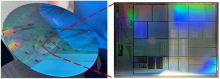
electrically pumped QD lasers grown by molecular beam epitaxy on a 300mm patterned (001) Si wafer with a butt-coupled
configuration. Unique growth and fabrication challenges imposed by the template architecture have been
resolved, contributing to continuous wave lasing to 60 °C and a maximum double-side output power of 126.6mW at
20 °C with a double-side wall-plug efficiency of 8.6%. The potential for robust on-chip laser operation and efficient low loss
light coupling to Si photonic circuits makes this heteroepitaxial integration platform on Si promising for scalable
and low-cost mass production.