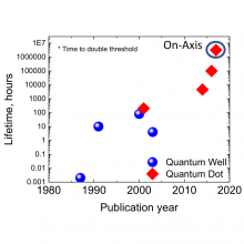
Direct epitaxial integration of III-V materials on Si offers substantial manufacturing cost and scalability advantages over heterogeneous integration. The challenge is that epitaxial growth introduces high densities of crystalline defects that limit device performance and lifetime. Quantum dot lasers, amplifiers, modulators, and photodetectors epitaxially grown on Si are showing promise for achieving low-cost, scalable integration with silicon photonics. The unique electrical confinement properties of quantum dots provide reduced sensitivity to the crystalline defects that result from III-V/Si growth, while their unique gain dynamics show promise for improved performance and new functionalities relative to their quantum well counterparts in many devices. Clear advantages for using quantum dot active layers for lasers and amplifiers on and off Si have already been demonstrated, and results for quantum dot based photodetectors and modulators look promising. Laser performance on Si is improving rapidly with continuous-wave threshold currents below 1 mA, injection efficiencies of 87%, and output powers of 175mWat 20 C. 1500-h reliability tests at 35 C showed an extrapolated mean-time-to-failure of more than ten million hours. This represents a significant stride toward efficient, scalable, and reliable III-V lasers on on-axis Si substrates for photonic integrate circuits that are fully compatible with complementary metal-oxidesemiconductor (CMOS) foundries.©2018 Author(s). All article content, except where otherwise noted, is licensed under a Creative Commons Attribution (CC BY) license (http://creativecommons.org/licenses/by/4.0/). https://doi.org/10.1063/1.5021345
