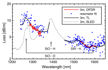
Ultra-low-loss waveguide fabrication typically requires high-temperature annealing beyond 1000◦C to reduce the hydrogen content in deposited dielectric films. However, realizing the full potential of an ultra-low loss will require the integration of active materials that cannot tolerate high temperature. Uniting ultra-low-loss waveguides with on-chip sources, modulators, and detectors will require a low-temperature, low-loss dielectric to serve as a passivation and spacer layers for complex fabrication processes. We report a 250◦C deuterated silicon dioxide film for top cladding in ultra-low-loss waveguides. Using multiple techniques, we measure propagation loss below 12 dB/m for the entire 1200–1650 nm range and top-cladding material absorption below 1 dB/m in the S, C, and L bands.