News Date
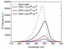
University of California Santa Barbara (UCSB) in the USA has been working to optimize gallium arsenide (GaAs) molecular beam epitaxy (MBE) on gallium phosphide on silicon (GaP/Si) [Daehwan Jung et al, J. Appl. Phys., vol122, p225703, 2017]. Normally, growth of GaAs on Si uses off-axis substrates in efforts to avoid anti-phase domains. On-axis silicon is preferred for compatibility with CMOS processing foundries. The lattice mismatch between GaAs and Si is ~4%, leading to dislocations.
News External Link
News Image