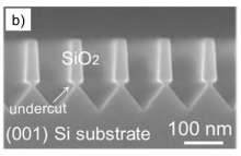
We report on the use of InGaAsP strain-compensated superlattices (SC-SLs) as a technique to reduce the defect density of Indium Phosphide (InP) grown on silicon (InP-on-Si) by Metal Organic Chemical Vapor Deposition (MOCVD). Initially, a 2 µm thick gallium arsenide (GaAs) layer was grown with very high uniformity on exact oriented (001) 300 mm Si wafers; which had been patterned in 90 nm V-grooved trenches separated by silicon dioxide (SiO2) stripes and oriented along the [110] direction. Undercut at the Si/SiO2 interface was used to reduce the propagation of defects into the III–V layers. Following wafer dicing; 2.6 µm of indium phosphide (InP) was grown on such GaAs-on-Si templates. InGaAsP SC-SLs and thermal annealing were used to achieve a high-quality and smooth InP pseudo-substrate with a reduced defect density. Both the GaAs-on-Si and the subsequently grown InP layers were characterized using a variety of techniques including X-ray diffraction (XRD); atomic force microscopy (AFM); transmission electron microscopy (TEM); and electron channeling contrast imaging (ECCI); which indicate high-quality of the epitaxial films. The threading dislocation density and RMS surface roughness of the final InP layer were 5 × 10⁸/cm2 and 1.2 nm; respectively and 7.8 × 10⁷/cm2 and 10.8 nm for the GaAs-on-Si layer.