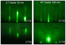
We report a systematic study of high quality GaAs growths on on-axis (001) GaP/Si substrates using molecular beam epitaxy. Various types of dislocation filter layers and growth temperatures of initial GaAs layer were investigated to reduce the threading dislocation densities in GaAs on GaP/Si. Electron channeling contrast imaging techniques revealed that an optimized GaAs buffer layer with thermal cycle annealing and InGaAs/GaAs dislocation filter layers has a threading dislocation density of 7.2 106 cm2 , which is a factor of 40 lower than an unoptimized GaAs buffer. The root-mean-square surface roughness was greatly decreased from 7.8 nm to 2.9 nm after the optimization process. A strong enhancement in photoluminescence intensity indicates that the optimized GaAs template grown on on-axis (001) GaP/Si substrates is a promising virtual substrate for Si-based optoelectronic devices.